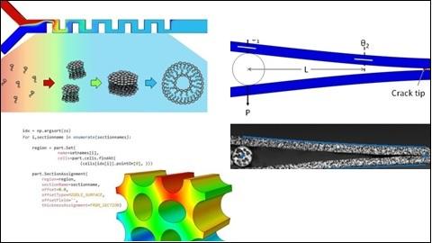
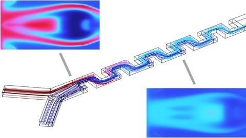
Veryst offers expertise in a full range of analytical tools and techniques for non-destructive and destructive failure analysis. Choosing the right analytical method is critical for determining the root cause of a failure. Some of the non-destructive methods we use begin with high magnification optical microscopy and scanning electron microscopy. Testing methods can include electrical, optical, mechanical, and acoustic testing.

Assembly Audits
Veryst performs assembly line audits of MEMS, sensors, and PCBA (printed circuit board assembly) manufacturing lines. Our audits include recommendations for improvements addressing processing, inspection, automation, yield, solder, and contamination, improving our clients' yield and reliability.
Surface Analysis
Failure mechanisms in sensors such as MEMS are often due to surface aberrations. MEMS have a high surface-area-to-volume ratio, and surface-related failure mechanisms such as stiction, wear, and charging are common in MEMS and sensors. Consequently, surface analysis techniques are particularly important for failure analysis of MEMS.
Veryst uses an array of highly sophisticated techniques for surface analysis. Scanning electron microscopy (SEM), interferometry, and atomic force microscopy (AFM) can provide detailed images of the surface of a failed part. Energy dispersive x-ray analysis (EDS), auger spectroscopy, Fourier transform infrared analysis (FTIR), x-ray photoelectron spectroscopy (XPS), time of flight secondary ion mass spectroscopy (TOFSIMS), and Raman spectroscopy provide surface elemental and chemical information. With all of these techniques, specimen preparation is critical and must be specific, clean, and accurate. Veryst is skilled with this process, and also understands the relative benefits of each of these techniques to collect the relevant surface data most efficiently. As with most analyses, tedious attention to detail will be rewarded with accurate and clean data.